Two years ago I assisted at a meeting at Elektor during which Software Defined Radio (SDR), GNU radio and its hardware platform the Universal Software Radio Peripheral (USRP) were discussed. The GNU radio people were really convincing and I liked the concept, but since then I didn't hear much of it. One of the reasons, I thought, was that the USRP (version 2 at the time) was quite an expensive platform.
During the visit of the University of Texas (UT) this morning a wireless class was presented that was based on SDR. The hardware platform was a PXI from National Instruments and the programming was done, of course, in LabVIEW. The goal of the course is to familiarise students with wireless concepts and instead of treating the subject only in a theoretical way, the UT decided to use an SDR hardware platform so that students can easily implement and try out the concepts in the real world. An excellent concept if you ask me.
Instead of keeping it a UT-only course they went a step further and developed an educational package that other schools and universities can buy from the UT. This package includes two now-where-did-I-see-you-before? USRPs (on the left in the photo). Actually, the USRP is now an NI product because NI bought Ettus Research in February 2010. I am afraid this will not really help to lower the price of the USRP.
I don't know if there is a difference between the USRP N210 that you can buy from Ettus and which looks identical to the USRP-2920 from NI, but maybe I can find that out this afternoon during the special USRP session?
Monday, August 1, 2011
In Texas everything is bigger
After having spent the sunday to get used to the what they allready call here the hottest summer ever (over 40 degrees Celsius for more than 50 days) today I will start attending NIWeek 2011. The show opens in less than one hour, but since it is just across the street I just have time to open the blog now.
My day will begin with a visit of the University of Texas (UT), the largest university of the USA as they say here in Austin with some 80,000 students. However, according to the internet, the UT is only the fifth university of the USA with just over 50,000 students. "In Texas everything is bigger" is another thing they like to say here. Apparently this holds true for claims too.
Stay tuned as there will be more to come.
My day will begin with a visit of the University of Texas (UT), the largest university of the USA as they say here in Austin with some 80,000 students. However, according to the internet, the UT is only the fifth university of the USA with just over 50,000 students. "In Texas everything is bigger" is another thing they like to say here. Apparently this holds true for claims too.
Stay tuned as there will be more to come.
Saturday, July 30, 2011
Smart phone, stupid protection
This morning (29/7) I took off from Schiphol (Amsterdam airport) for Austin, Texas to assist at the 17th NIWeek. During the flight I kept my phone switched off in a pocket of my pants. Now, when my phone is switched off the key lock function does not work because it is a function of the operating system of the phone, not a hardware feature. So, without me noticing, my phone got switched on in my pocket while I was looking out of the window (I had a window seat) and apparently I unknowingly sort of "punched" in (with my thigh or handkerchief) several wrong PIN codes which resulted in a blocked SIM card when I took my phone out again in Houston (where I had to change planes). To unblock the PIN code my phone now first wanted a Personal Unblocking Code (PUK) code, which off course I didn't know. A helpful girl in a phone shop on the airport told me that this code is often printed on the SIM card itself. So I examined my SIM card and indeed discovered a 17-digit code of which the first 8 digits turned out to be the PUK code for my SIM card. Great!
Or is it? Thanks to the missing hardware key lock feature my SIM card got blocked, but thanks to the PUK code conveniently printed on my SIM card, I can unblock it again. And if I can do this, anyone who gets hold of my phone can do this. How's that for anti-theft protection?
So, problem solved? Well... no. Entering the PUK code gave me the right to choose a new PIN code that I had to confirm by typing it again, which I did without errors. 1234 is not so difficult to get right, right? Wrong! According to my phone my new PIN code is incorrect (???) and I am back to the PUK code. I would now be stuck in an endless loop if it weren't for the cleverly built-in hang protection (they did think of that): the number of tries is limited to 8. I still have 3 left...
Tomorrow I will buy a prepaid local SIM card.
Or is it? Thanks to the missing hardware key lock feature my SIM card got blocked, but thanks to the PUK code conveniently printed on my SIM card, I can unblock it again. And if I can do this, anyone who gets hold of my phone can do this. How's that for anti-theft protection?
So, problem solved? Well... no. Entering the PUK code gave me the right to choose a new PIN code that I had to confirm by typing it again, which I did without errors. 1234 is not so difficult to get right, right? Wrong! According to my phone my new PIN code is incorrect (???) and I am back to the PUK code. I would now be stuck in an endless loop if it weren't for the cleverly built-in hang protection (they did think of that): the number of tries is limited to 8. I still have 3 left...
Tomorrow I will buy a prepaid local SIM card.
Wednesday, July 20, 2011
Vanity chips
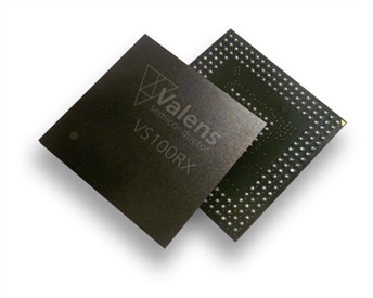
Have you ever heard of the company Valens Semiconductor? I hadn't either, until last night.
In 2009 Valens Semiconductor together with LG, Samsung and Sony announced their intention to launch a cross-industry alliance to promote and standardize the HDBaseT technology for whole-home distribution of uncompressed HD multimedia content. A few days later Valens announced the availability of an HDBaseT-compliant chipset: the VS100, consisting of the VS100TX transmitter and the VS100RX (receiver). This chipset enables the convergence of uncompressed full HD digital video, audio, 100BaseT Ethernet, power and control through a single, standard 100m/328ft LAN cable.
(I got this from their website)
To me this sounds like an interesting chipset (although a bit out of my league) for more than one reason. One of those reasons is the printing on the chip. Why?
Well, you may not know it, but my name is Valens. Before the era of internet my family and me knew of very few other people named Valens. There was of course Richie Valens, but that is not his real name, and there were some roman emperors named Valens (I have a coin to prove it). Now that the world population is massively coming on line more and more people and companies named Valens surface.
If you are an electronics engineer and your name happens to be National, Renesas or Avago you can easily find chips with your name on it, but for most other people such an opportunity is pretty rare. And I just came across one!
I want this chipset. Not for building something with it, but to keep on my desk. I want a vanity chip(set). Of course I have contacted the company and asked for a sample. If I get hold of one of these chips I will of course post it here.
In 2009 Valens Semiconductor together with LG, Samsung and Sony announced their intention to launch a cross-industry alliance to promote and standardize the HDBaseT technology for whole-home distribution of uncompressed HD multimedia content. A few days later Valens announced the availability of an HDBaseT-compliant chipset: the VS100, consisting of the VS100TX transmitter and the VS100RX (receiver). This chipset enables the convergence of uncompressed full HD digital video, audio, 100BaseT Ethernet, power and control through a single, standard 100m/328ft LAN cable.
(I got this from their website)
To me this sounds like an interesting chipset (although a bit out of my league) for more than one reason. One of those reasons is the printing on the chip. Why?
Well, you may not know it, but my name is Valens. Before the era of internet my family and me knew of very few other people named Valens. There was of course Richie Valens, but that is not his real name, and there were some roman emperors named Valens (I have a coin to prove it). Now that the world population is massively coming on line more and more people and companies named Valens surface.
If you are an electronics engineer and your name happens to be National, Renesas or Avago you can easily find chips with your name on it, but for most other people such an opportunity is pretty rare. And I just came across one!
I want this chipset. Not for building something with it, but to keep on my desk. I want a vanity chip(set). Of course I have contacted the company and asked for a sample. If I get hold of one of these chips I will of course post it here.
Wednesday, July 6, 2011
Control a robot with a watch
Some six months ago Texas Instruments announced the Evalbot, a development platform for their Stellaris ARM Cortex-M3 microcontrollers in the shape of a little robot. It took me a while to get hold of one, but now I have one driving happily around in my living room. It is actually a pretty neat and cleverly engineered kit that you have to assemble yourself. Most parts are made out of PCB material – the two wheels for instance are each made of three disks and a rubber ring – the rest are mainly nuts & bolts. Two little motors with gears drive the wheels and everything is powered from three AA batteries.
The Evalbot is not a gadget; it is a powerful development board with wheels. In the center off the disk-shaped board sits an LM3S9B92 ARM Cortex-M3 controller (256 KB flash, 96 KB RAM and more peripherals than you will probably ever need) assisted by a tiny 96 x 16 blue OLED display, 6 push-buttons (including the on/reset and the off buttons), an Ethernet connector, a USB host port, a USB device port, a USB debugger/programmer port (ICDI), a micro-SD card connector, a speaker, power supply, JTAG, two LEDs and probably more that I am overlooking now; and two motor drivers. Thanks to the battery holders (with batteries) on the bottom of the board the whole thing is pretty heavy and the rubber “tires” prevent sliding it off your desk when you hook the board up to a computer with a USB cable that wants to unwind the wrong way around.
A special wireless expansion port is available too on which you can plug a CC1101EM sub-1 GHz transceiver, which will get you an 868 or 915 MHz radio link. The James Bond part of this setup is a third kit from TI, the eZ430-Chronos based on the CC430F6137 sub-1 GHz RF SoC. This is a combination of a biggish but stylish black watch with a large character display and a USB access point for your PC. Once connected you can control your PC with the watch, although it takes some exercise to do it properly. But... you can also use the watch to control the Evalbot! An integrated accelerometer lets you influence the driving direction of the robot by tilting and rotating the watch. Cool huh? The watch in itself is actually a dev kit and you can reprogram it with your own application.
Programming the dev kits is done with Code Composer Studio 4, the Eclipse-based dev environment from TI. A license file is included with the Evalbot kit, but what exactly this enables is not clear to me. I did read something somewhere about code sizes & limits, but I forgot where. Anyway, all the source code for the Chronos controlled Evalbot is available, it compiles without warnings and errors and programs fine. This really is a fine (but strange) development kit.
The Evalbot is not a gadget; it is a powerful development board with wheels. In the center off the disk-shaped board sits an LM3S9B92 ARM Cortex-M3 controller (256 KB flash, 96 KB RAM and more peripherals than you will probably ever need) assisted by a tiny 96 x 16 blue OLED display, 6 push-buttons (including the on/reset and the off buttons), an Ethernet connector, a USB host port, a USB device port, a USB debugger/programmer port (ICDI), a micro-SD card connector, a speaker, power supply, JTAG, two LEDs and probably more that I am overlooking now; and two motor drivers. Thanks to the battery holders (with batteries) on the bottom of the board the whole thing is pretty heavy and the rubber “tires” prevent sliding it off your desk when you hook the board up to a computer with a USB cable that wants to unwind the wrong way around.
A special wireless expansion port is available too on which you can plug a CC1101EM sub-1 GHz transceiver, which will get you an 868 or 915 MHz radio link. The James Bond part of this setup is a third kit from TI, the eZ430-Chronos based on the CC430F6137 sub-1 GHz RF SoC. This is a combination of a biggish but stylish black watch with a large character display and a USB access point for your PC. Once connected you can control your PC with the watch, although it takes some exercise to do it properly. But... you can also use the watch to control the Evalbot! An integrated accelerometer lets you influence the driving direction of the robot by tilting and rotating the watch. Cool huh? The watch in itself is actually a dev kit and you can reprogram it with your own application.
Programming the dev kits is done with Code Composer Studio 4, the Eclipse-based dev environment from TI. A license file is included with the Evalbot kit, but what exactly this enables is not clear to me. I did read something somewhere about code sizes & limits, but I forgot where. Anyway, all the source code for the Chronos controlled Evalbot is available, it compiles without warnings and errors and programs fine. This really is a fine (but strange) development kit.
Labels:
ARM,
Cortex-M3,
Evalbot,
Stellaris,
Texas Instruments
Thursday, May 19, 2011
Intelligent simple peripherals
This week I once again wrote an interrupt service routine for a UART to do some serial communication. Actually I didn’t have to write a whole lot, because the receiver part had already been done by someone else, but the code for transmitting data under interrupt control was missing. I already had this code in another project and porting it was easy and quick, but then I started thinking.
Like me, probably thousands of programmers all over the world are doing this every day, which is a waste of time and resources. Of course we all try to reuse code as much as possible, but with micro-controllers getting more and more advanced, why don’t the silicon vendors simply implement the driver in the peripheral, in silicon? I mean, how many people do use the UART for other things than simply sending and receiving data? OK, we see more and more 16550 compatible UARTs, so drivers are easily found, but then again, why not put it in a ROM for the programmer’s convenience? All it has to do is to read data from a buffer and write data to it, all under interrupt control of course. An intelligent peripheral like that would save some code space, but most importantly, it would save lots of programmer’s time.
Such an intelligent peripheral would have a pretty simple interface: some registers to set up circular rx & tx buffers and the communication parameters, registers to read/write a block of data and some status registers to check for errors. The user only has to supply a block of RAM for the buffers. This is what most of us implement in our code anyway. For backward compatibility they should keep the traditional interface too, that way everything is possible.
Similar peripherals for other protocols could be integrated as well, like I2C or SPI.
The typical ISR for I2C is rather complicated and big, and is therefore prone to many bugs. Many software developers are struggling to get it working properly, so it would be a great service to them if the driver was already in the chip. I am not pleading for a full blown on-chip operating system, but some simple drivers that will take care of the most common tasks sure would be nice.
So you silicon vendors reading this please do give it a thought. I appreciate the integrated USB drivers, but don’t stop there. Why don’t you make things even better by adding hardcoded drivers for “simple” peripherals too?
Like me, probably thousands of programmers all over the world are doing this every day, which is a waste of time and resources. Of course we all try to reuse code as much as possible, but with micro-controllers getting more and more advanced, why don’t the silicon vendors simply implement the driver in the peripheral, in silicon? I mean, how many people do use the UART for other things than simply sending and receiving data? OK, we see more and more 16550 compatible UARTs, so drivers are easily found, but then again, why not put it in a ROM for the programmer’s convenience? All it has to do is to read data from a buffer and write data to it, all under interrupt control of course. An intelligent peripheral like that would save some code space, but most importantly, it would save lots of programmer’s time.
Such an intelligent peripheral would have a pretty simple interface: some registers to set up circular rx & tx buffers and the communication parameters, registers to read/write a block of data and some status registers to check for errors. The user only has to supply a block of RAM for the buffers. This is what most of us implement in our code anyway. For backward compatibility they should keep the traditional interface too, that way everything is possible.
Similar peripherals for other protocols could be integrated as well, like I2C or SPI.
The typical ISR for I2C is rather complicated and big, and is therefore prone to many bugs. Many software developers are struggling to get it working properly, so it would be a great service to them if the driver was already in the chip. I am not pleading for a full blown on-chip operating system, but some simple drivers that will take care of the most common tasks sure would be nice.
So you silicon vendors reading this please do give it a thought. I appreciate the integrated USB drivers, but don’t stop there. Why don’t you make things even better by adding hardcoded drivers for “simple” peripherals too?
Wednesday, May 4, 2011
FRAM - true unified memory
Somewhere in the beginning of 2007 I won in a lottery held by EPN magazine an evaluation board from Ramtron sporting their most powerful 8051 clone, the VRS51L3074, which could be programmed and debugged with a small USB piggyback board. The very special thing of the Ramtron controller was the 8 KB of non-volatile ferroelectric memory (F-RAM) it included.
Instead of putting the board in a box, I actually used it in a project. I used the F-RAM to store some parameters in. The evaluation board also had several other F-RAM chips on it, but I did not use those. Once the project finished (it was published in the January 2009 issue of Circuit Cellar) I (almost) forgot about F-RAM and never heard from Ramtron again.
This year at the Embedded World show in Nuremberg I again came across F-RAM, now spelled FRAM, at the Fujitsu stand. It turned out that they started licensing the technology from Ramtron and that they had put some of it in their MB95R family of 8-bit MCUs. Fujitsu also offers stand-alone FRAM devices up to 4 Mbit.
This week Texas Instruments announced their brand-new MSP430FR57xx family that includes up to 16 KB of FRAM, licensed at the same source. The people at TI are very excited about it and have high expectations for the future.
So what exactly is FRAM and why would you be excited about it?
The F in FRAM stands for ferroelectric (and not ferromagnetic nor Fujitsu) because it “uses ferroelectric film as a capacitor for storing data. Possessing characteristics of both ROM and RAM devices, FRAM features high speed access, high endurance in write mode, low power consumption, non-volatility, and excellent tamper resistance.” (Source: Fujitsu)
How it all works at the atomic level is not so important here, let’s jump to the bits interesting for people wanting to use FRAM in a design.
First there is speed. Compared to flash memory FRAM is way faster, TI claims a 100 times faster. According to Fujitsu, FRAM is 30,000 times faster than EEPROM.
Secondly, there is power consumption. FRAM uses very little power, 250 (TI) to 400 (Fujitsu) times less than flash or EEPROM. This is active power. Interestingly enough FRAM has a slightly higher leakage current than flash memory, so power consumption in sleep mode is slightly worse.
Less energy and higher speed means cost savings, not only on the power budget, but also on the production budget for the high-volume people that measure the time it takes to program a device on the production line.
Then there is endurance. Flash & EEPROM memory cells are specified for some 10,000 write cycles, whereas a FRAM memory cell can be rewritten more than a trillion times! (Fujitsu is a bit conservative here, TI rather optimistic.) This kind of endurance combined with the higher speed means that FRAM can be used in place of SRAM.
FRAM works with low programming voltages down to 1.5 V. Replacing a block of flash memory by a block of FRAM of the same density then saves die space because FRAM doesn’t need a charge pump. Smaller means cheaper. Also, because of the low programming voltage new applications become possible where the higher flash programming voltages are currently considered dangerous.
Finally, FRAM is less sensitive to external fields and alpha particles than flash memory because the memory cell capacitor’s dielectric is much thinner than the one of a flash memory cell. The thinner the dielectric the less distance there is to develop a dV over and the smaller are the chances to (accidentally) modify a bit.
All these advantages were known from the start, so why did it take so long before FRAM made its way into non-Ramtron MCUs? Well, I don’t know about Fujitsu, but according to TI the main reason was the incompatibility of the technology. Five years ago FRAM was done in 350 nm technology, which was too big to use it in TI’s chips. Now they brought it down to 130 nm, which is a perfect fit.

This is a picture of a demo board showing off the low-power capabilities of the new MSP430 family, targeted at energy harvesting applications. Battery backed SRAM, flahs or EEPROM can all be replaced by FRAM, the speed and low power requirements of FRAM make external super caps unnecessary. Higher speed equates to shorter up times so ultra-super-low-power applications seem to be ideal.
Since anyone can license this technology from Ramtron, we can expect other parts from other manufacturers to appear in the next months or years.
Jeez, why didn’t I buy Ramtron stock at the time when nobody cared?
Instead of putting the board in a box, I actually used it in a project. I used the F-RAM to store some parameters in. The evaluation board also had several other F-RAM chips on it, but I did not use those. Once the project finished (it was published in the January 2009 issue of Circuit Cellar) I (almost) forgot about F-RAM and never heard from Ramtron again.
This year at the Embedded World show in Nuremberg I again came across F-RAM, now spelled FRAM, at the Fujitsu stand. It turned out that they started licensing the technology from Ramtron and that they had put some of it in their MB95R family of 8-bit MCUs. Fujitsu also offers stand-alone FRAM devices up to 4 Mbit.
This week Texas Instruments announced their brand-new MSP430FR57xx family that includes up to 16 KB of FRAM, licensed at the same source. The people at TI are very excited about it and have high expectations for the future.
So what exactly is FRAM and why would you be excited about it?
The F in FRAM stands for ferroelectric (and not ferromagnetic nor Fujitsu) because it “uses ferroelectric film as a capacitor for storing data. Possessing characteristics of both ROM and RAM devices, FRAM features high speed access, high endurance in write mode, low power consumption, non-volatility, and excellent tamper resistance.” (Source: Fujitsu)
How it all works at the atomic level is not so important here, let’s jump to the bits interesting for people wanting to use FRAM in a design.
First there is speed. Compared to flash memory FRAM is way faster, TI claims a 100 times faster. According to Fujitsu, FRAM is 30,000 times faster than EEPROM.
Secondly, there is power consumption. FRAM uses very little power, 250 (TI) to 400 (Fujitsu) times less than flash or EEPROM. This is active power. Interestingly enough FRAM has a slightly higher leakage current than flash memory, so power consumption in sleep mode is slightly worse.
Less energy and higher speed means cost savings, not only on the power budget, but also on the production budget for the high-volume people that measure the time it takes to program a device on the production line.
Then there is endurance. Flash & EEPROM memory cells are specified for some 10,000 write cycles, whereas a FRAM memory cell can be rewritten more than a trillion times! (Fujitsu is a bit conservative here, TI rather optimistic.) This kind of endurance combined with the higher speed means that FRAM can be used in place of SRAM.
FRAM works with low programming voltages down to 1.5 V. Replacing a block of flash memory by a block of FRAM of the same density then saves die space because FRAM doesn’t need a charge pump. Smaller means cheaper. Also, because of the low programming voltage new applications become possible where the higher flash programming voltages are currently considered dangerous.
Finally, FRAM is less sensitive to external fields and alpha particles than flash memory because the memory cell capacitor’s dielectric is much thinner than the one of a flash memory cell. The thinner the dielectric the less distance there is to develop a dV over and the smaller are the chances to (accidentally) modify a bit.
All these advantages were known from the start, so why did it take so long before FRAM made its way into non-Ramtron MCUs? Well, I don’t know about Fujitsu, but according to TI the main reason was the incompatibility of the technology. Five years ago FRAM was done in 350 nm technology, which was too big to use it in TI’s chips. Now they brought it down to 130 nm, which is a perfect fit.

This is a picture of a demo board showing off the low-power capabilities of the new MSP430 family, targeted at energy harvesting applications. Battery backed SRAM, flahs or EEPROM can all be replaced by FRAM, the speed and low power requirements of FRAM make external super caps unnecessary. Higher speed equates to shorter up times so ultra-super-low-power applications seem to be ideal.
Since anyone can license this technology from Ramtron, we can expect other parts from other manufacturers to appear in the next months or years.
Jeez, why didn’t I buy Ramtron stock at the time when nobody cared?
Labels:
FRAM,
Fujitsu,
MSP430,
Ramtron,
Texas Instruments
Subscribe to:
Posts (Atom)