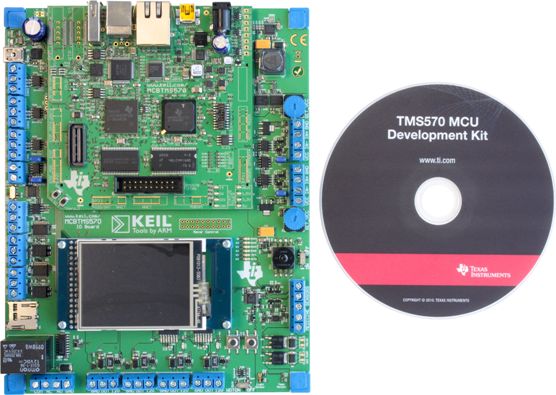
The other day a colleague asked me if I was interested in reviewing the TMS570 MCU Development Kit. This is a kit for playing with the TMS570LS20216 ARM Cortex-R4F microcontroller and when I looked at the picture of the kit available on the product page on TI web site I immediately became interested. It is a big main board with a TFT display and many connectors on which a smaller board sits. The TMS570 microcontroller is designed for use in safety critical systems and as such it includes [quote TI website] dual CPUs in lockstep, CPU and Memory Built-In Self Test (BIST) logic, ECC on both the Flash and the data SRAM, parity on peripheral memories, and loop back capability on peripheral I/O. The Floating Point CPU offers 1.6 DMIPS/MHz, and it has configurations which can run up to 160 MHz providing more than 250 DMIPS. [quote end] The TMS570LS20216 has 2 MB Flash memory and 160 KB SRAM. One might be tempted to say that this is a pretty powerful MCU.
When the kit to review arrived it turned out to be not exactly what I expected, as it was just a large USB stick. The stick is so large because otherwise the MCU in its 144LQFP package wouldn’t fit on it. It came in one of those CD/DVD boxes that we know from TI and that included besides the stick a little flash light, a DVD, a USB extension cable and a flyer with installation instructions. The installation instructions are simple: insert the DVD and do a full install. So I did.
I wrote down the amount of free disk space before launching the install and the time: 9h20. More than 30 minutes and 95 (really!) mouse clicks later the installation was complete. Looking at the free disk space left over I noticed that this demo had used a whopping 7 GB! As a comparison, my Windows XP Pro folder contains 9 GB. To be totally honest, I did this installation twice, the first time I just ran it while trying to do other things. But when the number of mouse clicks and the amazing amount of pop-up windows started bugging me I decided to redo the installation and count and measure the above mentioned parameters.
Naturally I now was pressed to see the demo's, curious to discover what a USB stick with only a few LEDs and a 5 square cm MCU on it supported by 7 GB of software had to offer. Connecting the stick to my PC worked fine, it was recognized immediately, and I started the Safety Demo Software as indicated in step 3 of the installation notes. A window with six large buttons came up and I clicked on the left upper one labelled “Safety Features”. The tool now first programmed the MCU before showing a block diagram of the chip and a list of small buttons on the left that let you generate an error event in the MCU. The error is graphically illustrated in the block diagram and a little red LED is lighted on the board.
You will have little trouble to understand that I was deeply impressed by this convincing demo so I quickly went on to try the others. I clicked the Ambient Light button and a little window with a vertical bar graph showing ambient light intensity came up. A light sensor included on the stick makes this demo possible. If you keep your hand over the stick the bar drops to a few percent and when you shine the flash light on the sensor you can get it up to 100%.
Again, Wow.
So quickly on to the next demo: the Temperature Sensor. Clicking the button opens a small window showing a graph of the temperature. According to the demo the temperature was over 30 degrees Celsius, at least 7 degrees higher than the ambient temperature, but maybe it measured closely to the MCU or the PC? Anyway, this demo was as convincing as the others.
What about the LED Light Show? Again a little window pops up and this time you can start the preprogrammed light show or toggle the six blue LEDs manually. To not spoil the surprise in case you want to buy this development stick yourself I will not tell you what happened but I can assure you that I was again deeply impressed.
If I remember correctly TI was the first to introduce the concept of USB development and evaluation sticks, but where the first one featured an MSP430 MCU that you could break off after programming and then use in your own application, this USB stick seems to be a pure product of marketing. Only 22 of the 144 pins (called “test points”) are brought out to two pin headers although a CAN bus is available too. You get a compiler too, so you can write some code for the MCU but do you really need 7 GB and 95+ mouse clicks for that?
Let us now define a benchmark for MCU development / evaluation kits so we can quickly compare the ease of use and system impact of those kits: the helloWorld (hW). The helloWorld is calculated as mds/(ds*(mc+i)) where “mds” is the highest capacity hard disk available in the year of release of the dev kit (see Wikipedia, in 2011 msb = 4 TB), “ds” stands for disk space needed by the dev kit and mc means mouse clicks needed to get an LED flashing on the dev kit and finally “i” is the number of icons & short-cuts created on the desktop (8 for this kit). With such a benchmark the flash light included in the kit would get a score of infinity because it does not occupy any disk space. The mds parameter is included to introduce an element of time in the benchmark so that it would be possible to compare helloWorld benchmarks over time. You might argue that including Eclipse in a dev kit should be a separate parameter pulling the score down, but Eclipse in itself consumes enough disk space to ensure a low benchmark anyway.
The TMS570 Microcontroller Development Stick presented here scores a value of 4 TB / 7 GB x (95 mouse clicks + 8 icons) = 5.68 helloWorld [hW].
If you have any suggestions of benchmark scores for other dev and or eval (evil?) kits, please do not hesitate to send them to me so I can publish them here.
Showing posts with label Texas Instruments. Show all posts
Monday, November 28, 2011
Tuesday, August 16, 2011
Wireless audio over 2.4 GHz
Just before the summer my contact at Texas Instruments had the excellent idea to sent me a CC85XXDK-HEADSET development kit. This is a PurePath Wireless Headset Development Kit to evaluate the new wireless audio products from TI based on the CC85xx family of RF micro-controllers. Due to a lack of time I didn't have the opportunity to write about it earlier, but I did give it a try and was impressed.
The kit contains two identical cards, one of which is configured as a master, the other as a slave. Both contain a 2.4 GHz radio and once paired (a simple operation) you can stream high quality stereo audio from the master to the slave. This works exceptionally well according to my non audiophile ears. The cards are each powered from one 1.72 Wh rechargeable li-ion battery, so it is a totally portable system. Charging the batteries is done by hooking the boards up to a USB port. TI claims a continues operation of 22 hours for this system.
I gave it a try in my garden and managed a Line of sight (LOS) distance of some 45+ meters (then I ran out of garden). It will probably go a bit further when the master is higher up from the ground. Occasionally the receiver has drop-outs, then it suddenly goes from full quality audio to complete silence, but this happens only at greater distances or when the data path becomes obstructed. Never did I hear any garbage out of the headphones.
Included in the kit is a little CC Debugger pod (with a funny rubbery feel) that you can use to reprogram the boards. This pod lets you reprogram and configure the boards using a tool called PurePath Wireless Configurator. The purpose of this tool is a bit unclear to me as there doesn't seem to be a whole lot that you can configure, but it is probably useful when you develop your own systems.
If you need a high quality wireless audio link in your system, the CC85xx is definitely worth a look!
The kit contains two identical cards, one of which is configured as a master, the other as a slave. Both contain a 2.4 GHz radio and once paired (a simple operation) you can stream high quality stereo audio from the master to the slave. This works exceptionally well according to my non audiophile ears. The cards are each powered from one 1.72 Wh rechargeable li-ion battery, so it is a totally portable system. Charging the batteries is done by hooking the boards up to a USB port. TI claims a continues operation of 22 hours for this system.
I gave it a try in my garden and managed a Line of sight (LOS) distance of some 45+ meters (then I ran out of garden). It will probably go a bit further when the master is higher up from the ground. Occasionally the receiver has drop-outs, then it suddenly goes from full quality audio to complete silence, but this happens only at greater distances or when the data path becomes obstructed. Never did I hear any garbage out of the headphones.
Included in the kit is a little CC Debugger pod (with a funny rubbery feel) that you can use to reprogram the boards. This pod lets you reprogram and configure the boards using a tool called PurePath Wireless Configurator. The purpose of this tool is a bit unclear to me as there doesn't seem to be a whole lot that you can configure, but it is probably useful when you develop your own systems.
If you need a high quality wireless audio link in your system, the CC85xx is definitely worth a look!
Wednesday, July 6, 2011
Control a robot with a watch
Some six months ago Texas Instruments announced the Evalbot, a development platform for their Stellaris ARM Cortex-M3 microcontrollers in the shape of a little robot. It took me a while to get hold of one, but now I have one driving happily around in my living room. It is actually a pretty neat and cleverly engineered kit that you have to assemble yourself. Most parts are made out of PCB material – the two wheels for instance are each made of three disks and a rubber ring – the rest are mainly nuts & bolts. Two little motors with gears drive the wheels and everything is powered from three AA batteries.
The Evalbot is not a gadget; it is a powerful development board with wheels. In the center off the disk-shaped board sits an LM3S9B92 ARM Cortex-M3 controller (256 KB flash, 96 KB RAM and more peripherals than you will probably ever need) assisted by a tiny 96 x 16 blue OLED display, 6 push-buttons (including the on/reset and the off buttons), an Ethernet connector, a USB host port, a USB device port, a USB debugger/programmer port (ICDI), a micro-SD card connector, a speaker, power supply, JTAG, two LEDs and probably more that I am overlooking now; and two motor drivers. Thanks to the battery holders (with batteries) on the bottom of the board the whole thing is pretty heavy and the rubber “tires” prevent sliding it off your desk when you hook the board up to a computer with a USB cable that wants to unwind the wrong way around.
A special wireless expansion port is available too on which you can plug a CC1101EM sub-1 GHz transceiver, which will get you an 868 or 915 MHz radio link. The James Bond part of this setup is a third kit from TI, the eZ430-Chronos based on the CC430F6137 sub-1 GHz RF SoC. This is a combination of a biggish but stylish black watch with a large character display and a USB access point for your PC. Once connected you can control your PC with the watch, although it takes some exercise to do it properly. But... you can also use the watch to control the Evalbot! An integrated accelerometer lets you influence the driving direction of the robot by tilting and rotating the watch. Cool huh? The watch in itself is actually a dev kit and you can reprogram it with your own application.
Programming the dev kits is done with Code Composer Studio 4, the Eclipse-based dev environment from TI. A license file is included with the Evalbot kit, but what exactly this enables is not clear to me. I did read something somewhere about code sizes & limits, but I forgot where. Anyway, all the source code for the Chronos controlled Evalbot is available, it compiles without warnings and errors and programs fine. This really is a fine (but strange) development kit.
The Evalbot is not a gadget; it is a powerful development board with wheels. In the center off the disk-shaped board sits an LM3S9B92 ARM Cortex-M3 controller (256 KB flash, 96 KB RAM and more peripherals than you will probably ever need) assisted by a tiny 96 x 16 blue OLED display, 6 push-buttons (including the on/reset and the off buttons), an Ethernet connector, a USB host port, a USB device port, a USB debugger/programmer port (ICDI), a micro-SD card connector, a speaker, power supply, JTAG, two LEDs and probably more that I am overlooking now; and two motor drivers. Thanks to the battery holders (with batteries) on the bottom of the board the whole thing is pretty heavy and the rubber “tires” prevent sliding it off your desk when you hook the board up to a computer with a USB cable that wants to unwind the wrong way around.
A special wireless expansion port is available too on which you can plug a CC1101EM sub-1 GHz transceiver, which will get you an 868 or 915 MHz radio link. The James Bond part of this setup is a third kit from TI, the eZ430-Chronos based on the CC430F6137 sub-1 GHz RF SoC. This is a combination of a biggish but stylish black watch with a large character display and a USB access point for your PC. Once connected you can control your PC with the watch, although it takes some exercise to do it properly. But... you can also use the watch to control the Evalbot! An integrated accelerometer lets you influence the driving direction of the robot by tilting and rotating the watch. Cool huh? The watch in itself is actually a dev kit and you can reprogram it with your own application.
Programming the dev kits is done with Code Composer Studio 4, the Eclipse-based dev environment from TI. A license file is included with the Evalbot kit, but what exactly this enables is not clear to me. I did read something somewhere about code sizes & limits, but I forgot where. Anyway, all the source code for the Chronos controlled Evalbot is available, it compiles without warnings and errors and programs fine. This really is a fine (but strange) development kit.
Labels:
ARM,
Cortex-M3,
Evalbot,
Stellaris,
Texas Instruments
Wednesday, May 4, 2011
FRAM - true unified memory
Somewhere in the beginning of 2007 I won in a lottery held by EPN magazine an evaluation board from Ramtron sporting their most powerful 8051 clone, the VRS51L3074, which could be programmed and debugged with a small USB piggyback board. The very special thing of the Ramtron controller was the 8 KB of non-volatile ferroelectric memory (F-RAM) it included.
Instead of putting the board in a box, I actually used it in a project. I used the F-RAM to store some parameters in. The evaluation board also had several other F-RAM chips on it, but I did not use those. Once the project finished (it was published in the January 2009 issue of Circuit Cellar) I (almost) forgot about F-RAM and never heard from Ramtron again.
This year at the Embedded World show in Nuremberg I again came across F-RAM, now spelled FRAM, at the Fujitsu stand. It turned out that they started licensing the technology from Ramtron and that they had put some of it in their MB95R family of 8-bit MCUs. Fujitsu also offers stand-alone FRAM devices up to 4 Mbit.
This week Texas Instruments announced their brand-new MSP430FR57xx family that includes up to 16 KB of FRAM, licensed at the same source. The people at TI are very excited about it and have high expectations for the future.
So what exactly is FRAM and why would you be excited about it?
The F in FRAM stands for ferroelectric (and not ferromagnetic nor Fujitsu) because it “uses ferroelectric film as a capacitor for storing data. Possessing characteristics of both ROM and RAM devices, FRAM features high speed access, high endurance in write mode, low power consumption, non-volatility, and excellent tamper resistance.” (Source: Fujitsu)
How it all works at the atomic level is not so important here, let’s jump to the bits interesting for people wanting to use FRAM in a design.
First there is speed. Compared to flash memory FRAM is way faster, TI claims a 100 times faster. According to Fujitsu, FRAM is 30,000 times faster than EEPROM.
Secondly, there is power consumption. FRAM uses very little power, 250 (TI) to 400 (Fujitsu) times less than flash or EEPROM. This is active power. Interestingly enough FRAM has a slightly higher leakage current than flash memory, so power consumption in sleep mode is slightly worse.
Less energy and higher speed means cost savings, not only on the power budget, but also on the production budget for the high-volume people that measure the time it takes to program a device on the production line.
Then there is endurance. Flash & EEPROM memory cells are specified for some 10,000 write cycles, whereas a FRAM memory cell can be rewritten more than a trillion times! (Fujitsu is a bit conservative here, TI rather optimistic.) This kind of endurance combined with the higher speed means that FRAM can be used in place of SRAM.
FRAM works with low programming voltages down to 1.5 V. Replacing a block of flash memory by a block of FRAM of the same density then saves die space because FRAM doesn’t need a charge pump. Smaller means cheaper. Also, because of the low programming voltage new applications become possible where the higher flash programming voltages are currently considered dangerous.
Finally, FRAM is less sensitive to external fields and alpha particles than flash memory because the memory cell capacitor’s dielectric is much thinner than the one of a flash memory cell. The thinner the dielectric the less distance there is to develop a dV over and the smaller are the chances to (accidentally) modify a bit.
All these advantages were known from the start, so why did it take so long before FRAM made its way into non-Ramtron MCUs? Well, I don’t know about Fujitsu, but according to TI the main reason was the incompatibility of the technology. Five years ago FRAM was done in 350 nm technology, which was too big to use it in TI’s chips. Now they brought it down to 130 nm, which is a perfect fit.

This is a picture of a demo board showing off the low-power capabilities of the new MSP430 family, targeted at energy harvesting applications. Battery backed SRAM, flahs or EEPROM can all be replaced by FRAM, the speed and low power requirements of FRAM make external super caps unnecessary. Higher speed equates to shorter up times so ultra-super-low-power applications seem to be ideal.
Since anyone can license this technology from Ramtron, we can expect other parts from other manufacturers to appear in the next months or years.
Jeez, why didn’t I buy Ramtron stock at the time when nobody cared?
Instead of putting the board in a box, I actually used it in a project. I used the F-RAM to store some parameters in. The evaluation board also had several other F-RAM chips on it, but I did not use those. Once the project finished (it was published in the January 2009 issue of Circuit Cellar) I (almost) forgot about F-RAM and never heard from Ramtron again.
This year at the Embedded World show in Nuremberg I again came across F-RAM, now spelled FRAM, at the Fujitsu stand. It turned out that they started licensing the technology from Ramtron and that they had put some of it in their MB95R family of 8-bit MCUs. Fujitsu also offers stand-alone FRAM devices up to 4 Mbit.
This week Texas Instruments announced their brand-new MSP430FR57xx family that includes up to 16 KB of FRAM, licensed at the same source. The people at TI are very excited about it and have high expectations for the future.
So what exactly is FRAM and why would you be excited about it?
The F in FRAM stands for ferroelectric (and not ferromagnetic nor Fujitsu) because it “uses ferroelectric film as a capacitor for storing data. Possessing characteristics of both ROM and RAM devices, FRAM features high speed access, high endurance in write mode, low power consumption, non-volatility, and excellent tamper resistance.” (Source: Fujitsu)
How it all works at the atomic level is not so important here, let’s jump to the bits interesting for people wanting to use FRAM in a design.
First there is speed. Compared to flash memory FRAM is way faster, TI claims a 100 times faster. According to Fujitsu, FRAM is 30,000 times faster than EEPROM.
Secondly, there is power consumption. FRAM uses very little power, 250 (TI) to 400 (Fujitsu) times less than flash or EEPROM. This is active power. Interestingly enough FRAM has a slightly higher leakage current than flash memory, so power consumption in sleep mode is slightly worse.
Less energy and higher speed means cost savings, not only on the power budget, but also on the production budget for the high-volume people that measure the time it takes to program a device on the production line.
Then there is endurance. Flash & EEPROM memory cells are specified for some 10,000 write cycles, whereas a FRAM memory cell can be rewritten more than a trillion times! (Fujitsu is a bit conservative here, TI rather optimistic.) This kind of endurance combined with the higher speed means that FRAM can be used in place of SRAM.
FRAM works with low programming voltages down to 1.5 V. Replacing a block of flash memory by a block of FRAM of the same density then saves die space because FRAM doesn’t need a charge pump. Smaller means cheaper. Also, because of the low programming voltage new applications become possible where the higher flash programming voltages are currently considered dangerous.
Finally, FRAM is less sensitive to external fields and alpha particles than flash memory because the memory cell capacitor’s dielectric is much thinner than the one of a flash memory cell. The thinner the dielectric the less distance there is to develop a dV over and the smaller are the chances to (accidentally) modify a bit.
All these advantages were known from the start, so why did it take so long before FRAM made its way into non-Ramtron MCUs? Well, I don’t know about Fujitsu, but according to TI the main reason was the incompatibility of the technology. Five years ago FRAM was done in 350 nm technology, which was too big to use it in TI’s chips. Now they brought it down to 130 nm, which is a perfect fit.

This is a picture of a demo board showing off the low-power capabilities of the new MSP430 family, targeted at energy harvesting applications. Battery backed SRAM, flahs or EEPROM can all be replaced by FRAM, the speed and low power requirements of FRAM make external super caps unnecessary. Higher speed equates to shorter up times so ultra-super-low-power applications seem to be ideal.
Since anyone can license this technology from Ramtron, we can expect other parts from other manufacturers to appear in the next months or years.
Jeez, why didn’t I buy Ramtron stock at the time when nobody cared?
Labels:
FRAM,
Fujitsu,
MSP430,
Ramtron,
Texas Instruments
Tuesday, February 16, 2010
Become a beta tester and win
It is contest time. I allready mentioned the Luminary, sorry, I mean Stellaris ARM contest from Texas Instruments together with Circuit Cellar and a week later the LPCXpresso ARM contest by NXP. Now it is Freescale who organises a contest. OK, this is not a very difficult contest and you don't have to design anything, but you can win some smart prizes.
To participate you only have to enter the CodeWarrior Development Studio 10.0 beta test program. Free access to the beta release, including full documentation and task-based videos are available for a limited time at www.freescale.com/cwmcu10. CodeWarrior integrates the development tools for the RS08, HCS08 and ColdFire architectures into a single product based on the Eclipse open development platform. Since this is a beta release, it cannot be used for the development of production products. However, you are encouraged to explore the functionality of this new development environment.
To recognize your participation, on April 12, 2010 Freescale will be drawing names from the pool of beta testers for three exciting prize packages:
- Canon Rebel digital single-lens reflex (SLR) camera
- Wii game console by Nintendo
- Garmin handheld GPS
So, go get that 500+ MB download and win that camera!
P.S. You have to submit feedback through a Freescale Service Request to really enter. Alternatively, participants may send an email with name, address (including zip code), home and work telephone numbers (including area codes) to r63076@freescale.com.
To participate you only have to enter the CodeWarrior Development Studio 10.0 beta test program. Free access to the beta release, including full documentation and task-based videos are available for a limited time at www.freescale.com/cwmcu10. CodeWarrior integrates the development tools for the RS08, HCS08 and ColdFire architectures into a single product based on the Eclipse open development platform. Since this is a beta release, it cannot be used for the development of production products. However, you are encouraged to explore the functionality of this new development environment.
To recognize your participation, on April 12, 2010 Freescale will be drawing names from the pool of beta testers for three exciting prize packages:
- Canon Rebel digital single-lens reflex (SLR) camera
- Wii game console by Nintendo
- Garmin handheld GPS
So, go get that 500+ MB download and win that camera!
P.S. You have to submit feedback through a Freescale Service Request to really enter. Alternatively, participants may send an email with name, address (including zip code), home and work telephone numbers (including area codes) to r63076@freescale.com.
Labels:
ARM,
codewarrior,
contest,
Freescale,
luminary,
NXP,
Stellaris,
Texas Instruments
Thursday, January 28, 2010
Will the new Bill Gates please stand up?
Circuit Cellar together with Texas Instruments have launched a design contest around the Stellaris LM3S9B96 microcontroller. This 100 pin controller is based on a 32-bit ARM Cortex–M3 core with 256 KB flash memory, 96 KB RAM and it sports many interesting features like CAN, USB 2.0 OTG/Host/Device, 10/100 Ethernet MAC and PHY, I2C, I2S, SSI, UART, PWM, ADC and some other peripherals. Although this is more or less what you would expect from a modern 32-bit microcontroller, it is not all: the device also has a built-in library with almost 400 functions to access its peripherals. This BIOS (Basic Input Output System) provides a nice hardware abstraction layer for almost all of the registers and makes life of the programmer much easier.
To top thing off, the device also has a built in real time operating system (RTOS)! According to the datasheet the controller has a copy of SafeRTOS inside, a secure version of FreeRTOS edited by Wittenstein. Unfortunately, the datasheet isn’t very verbose about it, but it is there.
Now what do you call a processor with peripherals, a BIOS and an operating system? A computer! Indeed, this microcontroller is pretty much like a computer on a chip (CoC) and the only thing missing is a graphical interface, but that is probably just a matter of time and/or pin count.
Are we entering a new era of microcontrollers? Will this be the new standard architecture for the next generation of microcontrollers? What about code portability? Will the user get access to the source code of the built-in BIOS and RTOS? Will ARM, TI & Wittenstein be the next Intel, AMD and Microsoft?
At the end of 2008 I assisted at an ARM conference in Paris. The buzz word then was "code portability". If only everybody would be using ARM-based processors, then code would be easily portable from one device to another. Luminary, the developper and former owner of the Stellaris processors, was present too. But is the BIOS & RTOS they now put in their devices good for code portability? Will other ARM-based microcontroller manufacturers too integrate a compatible BIOS & RTOS in their devices or provide compatible libraries? Or are we going to have to deal with tens of different BIOS-es and RTOS-es in the future, supported by code bloating tests to figure out what the heck the platform actually used is capable off?
Devices will get bigger and will integrate more and more. Within a couple of years they will be as powerfull as a modern PC is now, with built-in BIOS and OS. This all smells so much of Microsoft and the OS wars from the past years.
NOOOOOOOoooo!!!!!
Please, not again!
To top thing off, the device also has a built in real time operating system (RTOS)! According to the datasheet the controller has a copy of SafeRTOS inside, a secure version of FreeRTOS edited by Wittenstein. Unfortunately, the datasheet isn’t very verbose about it, but it is there.
Now what do you call a processor with peripherals, a BIOS and an operating system? A computer! Indeed, this microcontroller is pretty much like a computer on a chip (CoC) and the only thing missing is a graphical interface, but that is probably just a matter of time and/or pin count.
Are we entering a new era of microcontrollers? Will this be the new standard architecture for the next generation of microcontrollers? What about code portability? Will the user get access to the source code of the built-in BIOS and RTOS? Will ARM, TI & Wittenstein be the next Intel, AMD and Microsoft?
At the end of 2008 I assisted at an ARM conference in Paris. The buzz word then was "code portability". If only everybody would be using ARM-based processors, then code would be easily portable from one device to another. Luminary, the developper and former owner of the Stellaris processors, was present too. But is the BIOS & RTOS they now put in their devices good for code portability? Will other ARM-based microcontroller manufacturers too integrate a compatible BIOS & RTOS in their devices or provide compatible libraries? Or are we going to have to deal with tens of different BIOS-es and RTOS-es in the future, supported by code bloating tests to figure out what the heck the platform actually used is capable off?
Devices will get bigger and will integrate more and more. Within a couple of years they will be as powerfull as a modern PC is now, with built-in BIOS and OS. This all smells so much of Microsoft and the OS wars from the past years.
NOOOOOOOoooo!!!!!
Please, not again!
Thursday, December 10, 2009
And the winner is…
Last week I did a small survey of microcontroller preferences. Although I had an idea what to expect, there were some surprises in the responses. First of all I received much more reactions than I had hoped for. I would like to say thank you very much to all of you who took the time and effort to reply to this survey! The people that posted a reply (in English!) directly to the blog will find it added to my original post. Those that sent me an email, well, I am very sorry, I am not going to add them all to this blog as there were way, way too many. However, I did spend a few hours reading all the messages and a summary follows here.
What we all want to know now is of course: who won?
But before I will tell you, you will have to read through the following advertisement.
Just joking: the winner is… AVR! Yes, the AVRs received 43% of the votes, while the PIC family lagged behind with 35%. The rest of the votes went to other families of which the MSP430 and the Propeller were mentioned quite often. 8051/2 clones are also reasonably popular.
The main reason for the AVR domination was the available tools. Although free tools exist for many microcontrollers, BASCOM for AVR was mentioned several times and also Arduino. Now this survey originated at Elektor and was read mostly by Elektor readers, so it is biased as Elektor has published quite some projects using BASCOM-AVR, but in general it was felt that the free tools (BASCOM is free only for small executables) for AVR are better than those for PIC. Also the AVR seems to be more easily available and cheaper than a PIC (even more so since Microchip restricted their sampling program), especially important outside the US and Western Europe.
In favour of the PIC was the abundant documentation, examples and free libraries. It is true that Microchip puts a lot of effort in that. On a pure technical level, some people felt that the PIC is less sensitive to noise than the AVR.
Other processors were of course mentioned, but as the survey mainly spoke about PIC and AVR, most people restricted themselves to these two families. However, as stated by several people, if the MSP430 would exist in more DIP packages (only the smallest ones are available in DIP packages), they would definitely prefer it over both PIC and AVR. Surprisingly to me the Propeller from Parallax was mentioned a few times too. Personally I think of this processor more as a sort of freak processor and I would not easily invest time and money in it. Maybe the future proves me wrong, what do I know?
Several people liked the Stellaris, now from TI, others love Freescale.
What is very clear from all the responses and which didn’t surprise me much: architectural reasons clearly do not dominate the choice of a controller family. Once people have learned to use a certain microcontroller family and have invested in tools, they are not very likely to switch to another family from another manufacturer just for the fun of it.
So, my next question is: what does it take to make you switch to a competing microcontroller?
What we all want to know now is of course: who won?
But before I will tell you, you will have to read through the following advertisement.
Just joking: the winner is… AVR! Yes, the AVRs received 43% of the votes, while the PIC family lagged behind with 35%. The rest of the votes went to other families of which the MSP430 and the Propeller were mentioned quite often. 8051/2 clones are also reasonably popular.
The main reason for the AVR domination was the available tools. Although free tools exist for many microcontrollers, BASCOM for AVR was mentioned several times and also Arduino. Now this survey originated at Elektor and was read mostly by Elektor readers, so it is biased as Elektor has published quite some projects using BASCOM-AVR, but in general it was felt that the free tools (BASCOM is free only for small executables) for AVR are better than those for PIC. Also the AVR seems to be more easily available and cheaper than a PIC (even more so since Microchip restricted their sampling program), especially important outside the US and Western Europe.
In favour of the PIC was the abundant documentation, examples and free libraries. It is true that Microchip puts a lot of effort in that. On a pure technical level, some people felt that the PIC is less sensitive to noise than the AVR.
Other processors were of course mentioned, but as the survey mainly spoke about PIC and AVR, most people restricted themselves to these two families. However, as stated by several people, if the MSP430 would exist in more DIP packages (only the smallest ones are available in DIP packages), they would definitely prefer it over both PIC and AVR. Surprisingly to me the Propeller from Parallax was mentioned a few times too. Personally I think of this processor more as a sort of freak processor and I would not easily invest time and money in it. Maybe the future proves me wrong, what do I know?
Several people liked the Stellaris, now from TI, others love Freescale.
What is very clear from all the responses and which didn’t surprise me much: architectural reasons clearly do not dominate the choice of a controller family. Once people have learned to use a certain microcontroller family and have invested in tools, they are not very likely to switch to another family from another manufacturer just for the fun of it.
So, my next question is: what does it take to make you switch to a competing microcontroller?
Subscribe to:
Posts (Atom)